The vector triad results for the AMD Ryzen 1700X in my previous post allowed some interesting conclusions, but it is more instructive to compare them with a current Intel CPU. We have a desktop PC with an Intel “Skylake” Xeon E5-1275 v5 and dual-channel DDR4-2133 memory. This model was introduced in Q4/2015, and it does not support AVX-512 instructions. Although it has only four cores, it is a good fit because it has a similar price tag and power dissipation as the Ryzen 1700X, and it is also built with 14nm technology. The slightly lower theoretical memory bandwidth of 34.1 GB/sec does not really make a difference in practice.
The game is the same as before: I have fixed the clock frequency to 3.0 GHz, and the benchmark is the “throughput-mode vector triad”:
S = get_walltime()
do r=1,NITER
  do i=1,N
    A(i) = B(i) + C(i) * D(i)
  enddo
enddo
WT = get_walltime() - S
MFLOPS = 2.d0 * N * NITER / WT / 1.d6
This was run in parallel, without work sharing, on 1 to 4 cores. Again I have checked that FMA instructions make no difference whatsoever for this extremely data-bound code, and that likwid-bench delivers the same performance levels. An important architectural detail of the Skylake is worth mentioning: Just like its predecessors Haswell and Broadwell, it has a third address generation unit (AGU) for STOREs, hooked to execution port 7. In theory the core can thus sustain two AVX LOADs and one AVX STORE per cycle, doubling the per-cycle data throughput compared to Sandy Bridge and Ivy Bridge. However, Haswell and Broadwell had a limitation on this AGU: It could only process “simple” addresses, i.e., none of the complex addressing modes the Intel compiler uses by default (e.g., [rsi+8*rdx+32]) was able to use the AGU. The compiler (I tried up to version 17.0 update 2) does not know about this and refuses to choose simple addresses at least for the STOREs. By hacking the assembly code I could produce a version using simple addresses for the STOREs; see below for the consequences.
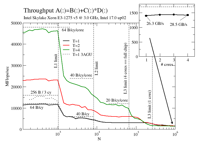
Throughput-mode vector triad on the Skylake chip vs. array length with 1, 2, and 4 cores. Inset: Performance for an in-memory dataset vs. number of cores. The bandwidth numbers assume a code balance of 20 B/flop in all hierarchy levels except L1.
The figure shows the results. I have chosen the same x and y axis ranges as in the Ryzen post, so the comparison should be straightforward:
In the L1 cache the data throughput is at 64 B/cy because the core can sustain either two AVX LOADs or one AVX LOAD and one AVX STORE per cycle. This proves that the third AGU at port 7 cannot be used with compiler-generated code. My “hacked” variant with simple addresses (only using [rcx] for the STOREs, shown as a dotted line) can get to the theoretical limit of 85.3 B/cy (not 96 because the bottleneck is the LOAD port – see any of our recent NLPE tutorials to understand why). But even without port 7 and AVX-512 the Skylake core can outperform the Ryzen by a factor of two per cycle. As a consequence, Skylake can reach the same L1 performance as Ryzen with four (or three, with some port 7 tweaking) instead of eight cores. Well, this was not entirely unexpected.
The large performance breakdown from L1 to L2 is characteristic of Intel architectures because of their “single-ported” L1 cache: In any given cycle, the cache can either talk to the registers or to the L2 cache, but not both. This “feature” was the starting point of our ECM performance model. On Skylake (and Broadwell) the increased L2 bandwidth of 64 B/cy, which was in theory available since Haswell, can actually be observed [1] (indirectly, of course, due to the non-overlapping L1). Despite its lower L1 performance, a Ryzen core can easily keep up with the Skylake because of its overlapping cache hierarchy. Due to its eight cores, the Ryzen 1700X has a massively better aggregate L2 performance, of course, and tops out at over 256 B/cy, whereas the Skylake chip stays at just below 160 B/cy.
The L3 cache on the Skylake is, as opposed to Ryzen, bandwidth-scalable up to all 4 cores. The Ryzen’s two “compute complexes” save its neck here because two L3s have two times the bandwidth, so the overall performance level is about 1.6x higher than on Skylake. One could argue that it is unfair to compare a four-core with an eight-core part, but I don’t actually care – this is not a bang-for-the-buck shootout but an architectural comparison.
The memory bandwidth (inset in the figure) shows similar characteristics to the Ryzen: A single core can almost saturate the bandwidth. Actually, if you let Turbo Mode do its thing there is hardly a discernible speedup in memory bandwidth for multiple cores. The Skylake achieves about 84% of the theoretical peak memory bandwidth for this benchmark. Just as on Ryzen, the efficiency goes up dramatically with a read-only benchmark and tops out at an impressive 97%.
Summing up, the Ryzen CPU cannot keep up with current Intel designs in terms of in-core performance with AVX(2) code. On the other hand, its overlapping cache hierarchy and good memory bandwidth (for a desktop chip) can regain a lot of lost ground despite the non-scalable L3 cache. I’m looking forward to the upcoming Naples CPU, although its value for HPC is probably questionable.
[1] J. Hofmann, D. Fey, M. Riedmann, J. Eitzinger, G. Hager, and G. Wellein: Performance analysis of the Kahan-enhanced scalar product on current multi- and manycore processors. Concurrency & Computation: Practice & Experience (2016). Available online, DOI: . Preprint: arXiv:1604.01890