We have recently acquired the brand-new AMD Ryzen 1700X (8 cores, 3.4+ GHz). Reading all the random numbers that people produce with their benchmarks made me sick, so I decided to run something that is well understood: The Schönauer vector triad. Everyone who knows our lectures and tutorials also knows this simple benchmark:
S = get_walltime()
do r=1,NITER
  do i=1,N
    A(i) = B(i) + C(i) * D(i)
  enddo
enddo
WT = get_walltime() - S
MFLOPS = 2.d0 * N * NITER / WT / 1.d6
Performance is reported in Mflops/sec for a wide range of problem sizes N, and NITER is chosen such that the benchmark runs for a sufficiently long time, long enough so that the wall-clock time measurement is accurate. On top of it we usually run the whole thing on different numbers of cores (using an OMP PARALLEL directive, but without worksharing on the inner loop) so we can evaluate the scalability of the different data paths without any adverse effects from OpenMP overhead. All this can be done very easily and efficiently using the likwid-bench microbenchmarking tool, but I have done the triad runs with my own Fortran-based code and checked afterwards that likwid-bench gives the same results.
The Ryzen system is equipped with 2x 16 GB of DDR4-2400 DRAM for a maximum theoretical memory bandwidth of 38.4 GB/sec. For the measurements I fixed the clock speed to 3.0 GHz, although the nominal clock speed is 3.4 GHz. The reason is simply my current inability to keep the CPU from running in Turbo mode when I set it to 3.4 GHz; it doesn’t matter for the benchmarks, though, because all in-cache numbers will be converted to bytes per cycle, and the memory bandwidth does not (significantly) depend on the clock frequency. I used the Intel compiler version 17.0 Update 2, which generates very decent AVX code on the chip if you give it the -Ofast -xHost options. Using FMAs would not make a difference because the Ryzen core executes a full-width 256-bit FMA in two chunks of 128 bits (and I have checked using likwid-bench that the FMA code runs exactly as fast as the non-FMA version). Besides, this code is totally bound by the data transfers even with data in the L1 cache. I have not used non-temporal store instructions; this is a topic for a future post.
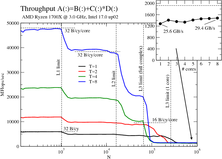
Throughput-mode vector triad on the Ryzen chip vs. array length with 1, 2, 4, and 8 cores. Inset: Performance vs. number of cores for an in-memory dataset. The bandwidth numbers assume a code balance of 20 B/flop in all hierarchy levels except L1.
Now for the data. The figure shows the usual stuff: Performance vs. array size for different numbers of threads (i.e., physical cores – SMT was ignored for this test). Here is my interpretation of the data:
With data in the L1 cache we get very close to 6 Gflops/sec per core, which amounts to a limit of 32 B/cy. Actually, the slide I stumbled across in the AMD booth at SC16 says “2 x 16B LOAD”, while another one says “2 LOADs & 1 STORE per cycle”. I don’t know how they want to sustain this with only two address generation units (AGUs), and the measured data is in line with a limit of “two 16-B LOADs OR one 16-B LOAD and one 16-B STORE per cycle,” identical to SSE limits on Intel Sandy Bridge and Ivy Bridge. If anyone can tell me how to get to the 8 Gflops/sec that can be expected if the 2LD+1ST story were true, go ahead. (Update: The two AGUs would be OK for one AVX LOAD and one half AVX STORE per cycle, just as on Sandy and Ivy Bridge; this would also lead to a maximum triad performance of 8 flops in 3 cycles. However, I can’t see it although the code is definitely AVX).
Between N=1024 and N=16384 the data comes from the 512 KiB per-core L2 cache. The drop in performance occurs at the same N independently of the core count, because we run the benchmark in “throughput mode”, i.e., with the same data size N on each core (think “weak scaling”). You can’t see it in the single-core data on this graph, but the 8-core runs tells us that the L2 actually delivers a little more than 32 B/cy. I have assumed here that there is a write-allocate for every store miss in the L1, increasing the code balance from 16 B/flop to 20 B/flop. The AMD slides linked above are a little cloudy on the details, they only state “32 B/cy” above two arrows between L1 and L2, so it isn’t clear whether this is 32 B/cy per direction or not. Another explanation could be that the write-allocate is optimized away by the hardware if it detects in its line fill buffers a write miss on a cache line that will be completely overwritten. We don’t know for sure, but once likwid-perfctr is ported to the architecture it should be able to shed some light on this.
Another important observation about the L2 (and also the L3): Data transfers overlap quite efficiently with retired LOADs in the L1. If you know the ECM performance model [1] you know that this is not at all the case on current Intel CPUs, making the AMD caches very effective (the IBM Power8 also behaves like this [2]).
The L3 cache is not core-local, but 8 MiB of shared L3 are available to each of the two four-core “core complexes” (CCX). The data clearly reflects this organization: Since I have pinned the threads in core order, i.e., filling one CCX first and then the other, this means we observe a performance drop beyond N=218 on a single core and beyond N=216 on the four cores of one CCX. Nothing changes from four to eight, however, because we get another 8 MiB of L3.
The most important observation about the L3 cache is that its bandwidth does not scale from one to four cores. There is only a slight speedup from 2 to 4, and it tops out at slightly above 64 B/cy assuming a code balance of 20 B/flop. The L3 is also a victim cache, i.e., only cache lines overflowing from the higher-level caches end up there. We will see how the efficiency of the L3 can be influenced by optimizations (such as, e.g., prefetch instructions, which I haven’t used at all here). The L3 bandwidth scales, of course, from 4 to 8 cores simply because there are two L3s.
Finally, the memory bandwidth behavior. This chip has the (IMO very attractive) property that a single core can almost saturate the memory bandwidth of the full chip. Intel desktop CPUs (but not the Xeons) behave in a similar way. The inset in the figure shows performance vs. number of cores for large N. The best bandwidth on a single CCX is obtained with two cores, and there is a slight drop for 3 and 4. We may speculate that this is a faint echo of the non-scalable L3 cache, but there may be many other reasons. With all eight cores we top out at just below 30 GB/sec, which is 77% of the theoretical memory bandwidth (dashed line in the inset). A read-only benchmark yields almost 90%, so it seems that the Ryzen also shares this feature with current Intel chips: the more read-dominated the code, the closer we can get to the peak memory bandwidth. The best overall chip bandwidth is obtained with two threads, one running on each CCX.
My next post will show the same test on a Skylake-type chip for comparison.
[1] H. Stengel, J. Treibig, G. Hager, and G. Wellein: Quantifying performance bottlenecks of stencil computations using the Execution-Cache-Memory model. Proc. ICS15, the 29th International Conference on Supercomputing, June 8-11, 2015, Newport Beach, CA. DOI: 10.1145/2751205.2751240. Preprint: arXiv:1410.5010
[2] J. Hofmann, D. Fey, M. Riedmann, J. Eitzinger, G. Hager, and G. Wellein: Performance analysis of the Kahan-enhanced scalar product on current multi- and manycore processors. Concurrency & Computation: Practice & Experience (2016). Available online, DOI: . Preprint: arXiv:1604.01890