Everyone’s got their pet peeves: For Poempelfox it’s Schiphol Airport, for Andreas Stiller it’s the infamous A20 gate. Compared to those glorious fails, my favorite tech blunder is a rather measly one, and it may not be relevant to many users in practice. However, it’s not so much the importance of it but the total mystery of how it came to happen. So here’s the thing.
Loads, stores, and AGUs
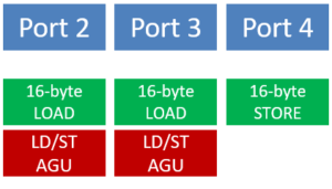
The Intel Sandy Bridge and Ivy Bridge architectures have six execution ports, two of which (#2 & #3) feed one LOAD pipeline each and one (#4) feeds a STORE pipe. These units are capable of transferring 16 bytes of data per cycle each. With AVX code, the core is thus able to sustain one full-width 32-byte LOAD (in two adjacent 16-byte chunks) and one half of a 32-byte STORE per cycle. But the LOAD and STORE ports are not the only thing that’s needed to execute these instructions – the core must also generate the corresponding memory addresses, which can be rather complicated. In a LOAD instruction like:
vmovupd ymm0, [rdx+rsi*8+32]
the memory address calculation involves two integer add operations and a shift. It is the task of the address generation units (AGUs) to do this. Each of ports 2 and 3 serves an AGU in addition to the LOAD unit, so the core can generate two addresses per cycle – more than enough to sustain the maximum LOAD and STORE throughput with AVX.
The peculiar configuration of LOAD and STORE units and AGUs causes some strange effects. For instance, if we execute the Schönauer vector triad:
A(:) = B(:) + C(:) * D(:)
with AVX on Ivy Bridge, it is clearly LOAD bound with a maximum in-core throughput of one AVX iteration in 3 cycles, i.e., 8/3 flop/cy. The three LOADs take three cycles, the STORE needs two, the arithmetic can be done in one, and the AGUs are not even 100% busy since we only require 4 addresses every 3 cycles. The compiler typically employs sufficient unrolling on top of AVX to reduce the overhead of the “loop mechanics” to nil. On our Ivy Bridge I can measure up to 98% of the theoretical limit with a working set that fits into L1 (992 elements per array).
However, with SSE (16-byte wide) instructions, the game is different: The LOAD ports now act independently, each requiring an address to execute a LOAD. The STORE port can issue one 16-byte STORE per cycle, so in principle it should be possible to execute two LOADs and one STORE per cycle, and there may even be room for another instruction before we hit the absolute limit of four micro-ops per cycle. However, with only two AGUs, that’s impossible: The core can either do two LOADs or one LOAD and one STORE per cycle. The Schönauer triad will thus execute in two cycles per SSE iteration, or 2 flop/cy, which is also easily in reach with compiler-generated code. Neither the LOAD nor the STORE units are continuously busy, and the bottleneck is actually the AGUs’ throughput. As a consequence, the AVX code is only a factor of 4/3 faster than the SSE version (and 8/3 times faster than the scalar code, for that matter), although the SIMD width alone makes a different promise.
The port 7 AGU on Haswell
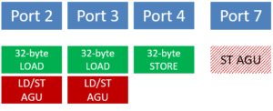
It is not uncommon that AGUs limit the throughput of LOAD and STORE units. The Marvell ThunderX2 has the same number of (16-byte) LOAD and STORE ports and the same number of AGUs as the Ivy Bridge, leading to the same limitations. AMD Zen? Same story. But if major improvements are made to the L1 bandwidth, the AGUs may quickly become an annoying bottleneck. In the Haswell architecture, Intel doubled the bandwidth of the L1, which could now sustain two 32-byte LOADs and one 32-byte STORE per cycle. The LOAD and STORE units’ widths were correspondingly doubled to match this, but with two AGUs it would never have been possible to attain this limit. Hence it is not surprising that a third AGU was added in Haswell. It has all of the new port 7 to itself and is responsible for generating STORE addresses only (the AGUs on the LOAD ports can serve LOADs and STOREs alike). With three AGUs a Haswell core should be able to run the Schönauer triad at 1.5 cy per AVX2 iteration, or 16/3 flop/cy.
Alas! It is not. Whatever you do, compiler-generated code (perfect as it may appear) only runs at 4 flop/cy, i.e., 2 cy per AVX2 iteration. This is the generated assembly code (Intel 19.02, options -Ofast -xAVX2):
..B2.8:
  vmovupd ymm2, [r13+r8*8]
  vmovupd ymm4, [32+r13+r8*8]
  vmovupd ymm6, [64+r13+r8*8]
  vmovupd ymm8, [96+r13+r8*8]
  vmovupd ymm1, [r12+r8*8]
  vmovupd ymm3, [32+r12+r8*8]
  vmovupd ymm5, [64+r12+r8*8]
  vmovupd ymm7, [96+r12+r8*8]
  vfmadd213pd ymm2, ymm1, [rsi+r8*8]
  vfmadd213pd ymm4, ymm3, [32+rsi+r8*8]
  vfmadd213pd ymm6, ymm5, [64+rsi+r8*8]
  vfmadd213pd ymm8, ymm7, [96+rsi+r8*8]
  vmovupd [r14+r8*8], ymm2
  vmovupd [32+r14+r8*8], ymm4
  vmovupd [64+r14+r8*8], ymm6
  vmovupd [96+r14+r8*8], ymm8
  add r8, 16
  cmp r8, r9
  jb ..B2.8
Nothing out of the ordinary here: The compiler has unrolled the loop four times on top of AVX2, which requires the core to execute the 19 instructions in 4\times1.5=6 cycles in order to attain the theoretical maximum. I’ve taken care to align the arrays to cache line boundaries, so any residual split cache line load penalty does not apply. So what’s going on here? (If you think “So what? 2 instead of 1.5 cycles? In L1? Who cares?”, you may be right. But that’s not the point here. Go away and leave the bean counters alone.)
There is a slight hint in Table 2-14 of the September 2019 Intel 64 and IA32 Architectures Optimization Reference Manual: It lists a “Simple_AGU” connected to port 7. Some more digging in Agner‘s forum and eventually asking an Intel representative got me the answer. The AGU behind port 7 can only handle “simple” addressing modes, more specifically, those of the form [BASE+OFFSET]. Using an index register is ruled out. The compiler (almost) always uses indexed addressing, so the port 7 AGU is never used and we’re back to two AGUs.
“Optimized” assembly
Hacking the assembly to check this hypothesis is easy (changes highlighted):
  push r14
..B2.8:
  vmovupd ymm2, [r13+r8*8]
  vmovupd ymm4, [32+r13+r8*8]
  vmovupd ymm6, [64+r13+r8*8]
  vmovupd ymm8, [96+r13+r8*8]
  vmovupd ymm1, [r12+r8*8]
  vmovupd ymm3, [32+r12+r8*8]
  vmovupd ymm5, [64+r12+r8*8]
  vmovupd ymm7, [96+r12+r8*8]
  vfmadd213pd ymm2, ymm1, [rsi+r8*8]
  vfmadd213pd ymm4, ymm3, [32+rsi+r8*8]
  vfmadd213pd ymm6, ymm5, [64+rsi+r8*8]
  vfmadd213pd ymm8, ymm7, [96+rsi+r8*8]
  vmovupd [r14], ymm2
  vmovupd [32+r14], ymm4
  vmovupd [64+r14], ymm6
  vmovupd [96+r14], ymm8
  add r14, 128
  add r8, 16
  cmp r8, r9
  jb ..B2.8
  pop r14
Now all stores use only [BASE+OFFSET] addressing. Register r14, the base address of the target array, must be updated within the loop, and to make it compatible with the surrounding mumbo-jumbo (remainder loops and such) I save it on the stack before the loop and restore it afterwards.
Running this code I could observe two things: (1) The performance is now consistently above 4 flop/cy, so obviously the two-AGU limit must have been overcome, and (2) although some runs attain up to 92% of the 16/3 flop/cy limit, there is a considerable run-to-run variation in the order of 5%. One can only speculate that sometimes the STORE address generation still happens on port 2 or 3 but the LOAD addresses cannot come from the port 7 AGU. Intel’s documents provide no insight here, but LIKWID does:
$ likwid-perfctr -C 1 -g UOPS_EXECUTED_PORT_PORT_7:PMC1,AVX_INSTS_CALC:PMC2 ./a.out
This counts overall AVX computation instructions (of sorts; see this for details) and the number of µops on port 7. It turns out that low performance is strongly correlated with a lower utilization of port 7, and whenever performance is good the two numbers are very close together. I’d love to study this more quantitatively, but this is something for a future post.
Long story short, port 7 cannot handle indexed addressing, and the compiler doesn’t give a s#!t. I’ve seen it generate LEA instructions sometimes, but I have no idea about the heuristics behind that. See also this post for some more detailed info on which instructions cannot be handled, address-wise, by port 7.
Broadwell, Skylake, Cascade Lake, and the future
There is not much more to say. All Intel architectures from Haswell to Cascade Lake have the simple AGU problem at port 7. On Skylake and Cascade Lake, the LOAD/STORE throughput doubles anyway because of the 64-byte SIMD width, but the unmodified, compiler-generated (don’t forget the “secret weapon” -qopt-zmm-usage=high) Schönauer triad is still AGU bound. The next new thing will be Ice Lake, but I still have to get my hands on one of those. The September 2019 optimization manual has a section 2.1 about Ice Lake, which states that new ports 8 and 9 will be serving a new store address AGU and another STORE unit, respectively. No mention of “simple addresses,” but also no clear statement about AGU capabilities.
Why?
What’s a total mystery to me is why Intel chose to build an AGU that cannot handle all kinds of addresses. In 2017, it was indicated to me that there “was not enough space on the die.” I find this hard to believe, especially because the problem prevailed in (at least) three further generations of Intel CPUs after Haswell. Maybe we’ll never know.
And finally, again, it’s a pet peeve. If you find this to be of any relevance to actual applications, I’ll be happy to hear from you.

