Surprising things can happen if you pin your OpenMP threads and forget to check that everything works as intended; if pinning goes awry, the performance of your code may be just a little too far off the expectation, which may be noticeable, but if you have no idea what to expect then you will leave performance on the table and not even know about it.
The case
In a recent case we came across, the user had compiled a hybrid MPI+OpenMP code. For node-level benchmarking he started the binary without mpirun or mpiexec and used likwid-pin to bind threads to cores:
$ likwid-pin -C N:0-27 ./a.out
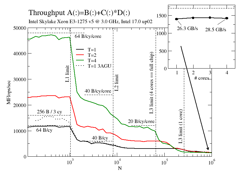
It was a memory-bound code, and performance seemed OK at first (one could observe the typical saturation pattern with increasing core count), but the saturated performance was about 25% below the Roofline limit, a little too slow to attribute it so some machine quirk. Of course we made sure that the Roofline model used the correct computational intensity, and that the memory bandwidth was derived from a reasonable STREAM measurement. 25% may not seem much, but in such a situation (and on a well-known architecture like the Intel Broadwell EP) it is often worthwhile to try and find out what’s going on – probably we can learn something new along the way.
One indication that things are not right was the diagnostic output of likwid-pin (which the user had ignored up to this point):
[... SNIP ...]
     threadid 140314618013440 -> core 26 - OK
     threadid 140314413209344 -> core 27 - OK
 Roundrobin placement triggered
     threadid 140314208405248 -> core 0 - OK
     threadid 140314003601152 -> core 1 - OK
     threadid 140314003601002 -> core 2 - OK
The “Roundrobin placement triggered” message should never show up. It means that more threads were spawned than the pin mask could accommodate. If you want to conduct a very special experiment, that may be what you want, but in general it isn’t. likwid-pin has those nice diagnostic messages, so it’s actually quite easy to see, but if you use some other affinity mechanism (or the -q switch with likwid-pin) then you must use some other means of checking. The “top” tool comes to mind: Many users don’t know that it can be configured to (i) show individual threads of a running binary (by hitting “H”), (ii) display the core each thread or process is running on (by hitting “f” and selecting “Last CPU used” as a display column), and (iii) to display the utilization of individual cores (by hitting “t” repeatedly, cycling through several display options). This way one could have noticed that the code above always left core 3 idle, although the pin mask definitely included it, and that core 0 was running two application threads in time-sharing mode. Note also that if we had used OMP_NUM_THREADS to set a smaller thread count (e.g., 14) but left the pin mask as it is, the “Roundrobin” message would not have shown up since the pin mask would have had ample space for the extra threads. This is a common scenario when doing intra-node scaling tests.
Shepherd Threads
So what was going on? To understand this we have to learn about shepherd threads. These are threads that are generated by your program, or rather the runtime underneath your chosen programming model, to work some under-the-hood magic. For instance, the Intel compilers up to version 17 Update 0 used a single shepherd for OpenMP. When your code hit the first parallel OpenMP region (this is where usually the application threads are brought to life), the runtime generated an extra thread first (i.e., as the first newly spawned thread after the master). There is no documentation about what this thread is for, but we have indications that it is at least used for waking up the team of threads after they went to sleep in a barrier. The important thing is, however, that the shepherd does not execute any user code, nor does it use any significant CPU time.
This is why likwid-pin sometimes displays a “SKIP SHEPHERD” message:
[... SNIP ...]
[pthread wrapper]
[pthread wrapper] MAIN -> 0
[pthread wrapper] PIN_MASK: 0->1 1->2 2->3 3->4 4->5 5->6 6->7 7->8 8->9
[pthread wrapper] SKIP MASK: 0x0
   threadid 139941087876864 -> SKIP SHEPHERD
   threadid 139941064513408 -> core 1 - OK
[... SNIP ...]
likwid-pin tries to figure out automatically if a newly generated thread is a shepherd. If it is, no pinning takes place, and it is left to roam around freely in the machine. When Intel dumped the shepherd thread in their 17.0 Update 1 compiler, this gave the developers some headache, and the code for shepherd detection had to be adapted. As of LIKWID 4.3, likwid-pin (and, of course, likwid-mpirun and likwid-perfctr) can reliably detect shepherds with all Intel compilers. The GCC compilers do not use shepherds at all (as of today), and LIKWID handles that, too.
What’s all the fuss about then? Well, shepherds are still something to be reckoned with, and they are typically not well documented. In our introductory example, the user had used g++ with OpenMPI and asynchronous progress enabled. It turned out that, although g++ itself did not spawn a shepherd, OpenMPI did: It spawned three, to be precise. In the hybrid MPI+OpenMP program, these three extra threads were generated after the main thread. This is why likwid-pin complained about “Roundrobin” placement, and this is also why core 3 was idle and core 0 was overloaded. Core 0 was running the OpenMP master, cores 0-2 were running the last three user threads, cores 1 and 2 were additionally running two shepherds (with no adverse effects), while core 3 had only the third shepherd to tend to. OpenMPI is not the only MPI implementation to use shepherds. Intel MPI has them, too, and what’s worse, their number depends on whether you use intra-node communication only or not. LIKWID does its best to detect the shepherds, but ultimately the only way to be sure that everything is OK is to check it using, e.g., “top.”
The LIKWID skip mask
If likwid-pin cannot figure out the shepherds correctly, you can still do it on your own and instruct the tool to ignore specific threads for pinning. This is what the skip mask is for. It is a hex code in which each bit represents a thread (excluding the master). For example, if you know that for some reason you have three shepherds, all generated right after the master thread, you would call likwid-pin (and all other LIKWID tools that do affinity) with the -s option and a hex argument:
$ likwid-pin -C N:0-27 -s 0x7 ./a.out
This will lead to three “SKIP SHEPHERD” messages after the master thread is pinned, and subsequent threads will be pinned according to the given mask. In the case described above, this option fixed the problem, eliminated the “Roundrobin” warning, and led to an outright 30% increase in performance because core 0 now had the same workload as everyone else.
Note that the shepherd thing can go either way performance-wise. Imagine you have a large skip mask covering all cores in a ccNUMA system, the shepherds are not detected correctly, and you use OMP_NUM_THREADS to run a team that spans a single ccNUMA domain only – or so you thought. Instead, the shepherd(s) are pinned to cores on the first domain, and the last couple of threads go to the second domain. Voilà: more bandwidth for everyone, and thus more performance than what Roofline on one domain would allow.
The gist of it is, if you use some affinity mechanism, check that it works as intended in your environment. If you change the compiler or the MPI implementation, check again. Note also that correct pinning can be a challenge for hybrid MPI+OpenMP programs. This is why we have likwid-mpirun. And finally, it goes without saying that a performance model really helps with figuring out such issues. As an added bonus, it gives you good karma.